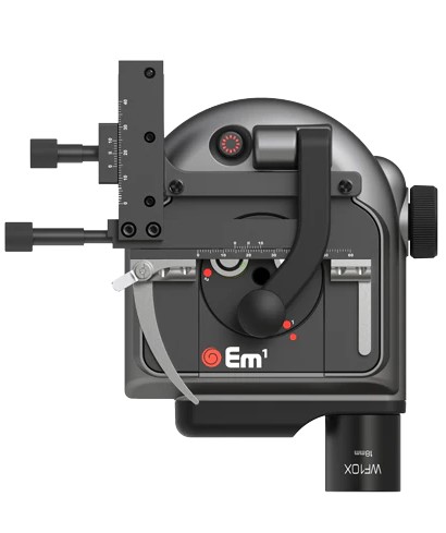
Scanning Electron Microscope (SEM): Exploring the Micro World in Detail

A Scanning Electron Microscope (SEM) is a powerful imaging tool that uses a focused beam of electrons instead of light to produce high-resolution, three-dimensional-like images of a sample’s surface. SEM technology has transformed research in materials science, biology, electronics, forensics, and countless other fields by allowing scientists to observe structures at the nanometer scale.
How a Scanning Electron Microscope Works
In SEM, a beam of electrons scans across the surface of the sample in a raster pattern. When the electrons interact with the atoms on the surface, they produce signals such as secondary electrons, backscattered electrons, and X-rays. These signals are then detected and converted into detailed images. The result is an incredibly sharp view of a specimen’s texture, shape, and composition.
One of the unique strengths of SEM is its depth of field, which gives images a three-dimensional appearance. This makes SEM invaluable for understanding surface features and fine details that conventional light microscopes cannot capture.
Applications of SEM
The versatility of SEM makes it a key tool across various industries and research areas:
- Materials Science – Examining metals, polymers, ceramics, and composites for structural integrity and failure analysis.
- Biology & Life Sciences – Studying microorganisms, tissues, and cell surfaces with exceptional clarity.
- Electronics – Inspecting microchips, circuit boards, and nanostructures for defects and quality control.
- Forensics – Analyzing trace evidence like gunshot residues, fibers, and soil samples for criminal investigations.
- Archaeology & Geology – Understanding the composition and surface morphology of fossils, minerals, and artifacts.
Advantages of Scanning Electron Microscopy
- High Resolution: SEM can magnify up to 1,000,000x, revealing nanoscale details.
- 3D-Like Imaging: Its large depth of field provides a more realistic representation of samples.
- Elemental Analysis: When combined with Energy Dispersive X-ray Spectroscopy (EDS), SEM can provide information on a sample’s chemical composition.
- Versatility: Suitable for both organic and inorganic materials, from biological tissues to industrial metals.
Limitations to Consider
While SEM offers exceptional imaging capabilities, it requires careful sample preparation, often involving coating non-conductive specimens with a thin layer of conductive material like gold or carbon. Additionally, SEM instruments are large, expensive, and require controlled laboratory conditions to operate effectively.
The Future of SEM Technology
Recent advancements in SEM technology aim to make these systems faster, more automated, and capable of working with more delicate samples without extensive preparation. Portable and tabletop SEM units are also emerging, making this technology more accessible to smaller laboratories, educational institutions, and even field research.
Conclusion
The Scanning EM Microscope remains one of the most essential tools in modern science, offering unparalleled insights into the microscopic world. Whether it’s uncovering the intricate details of a butterfly wing or analyzing the microstructure of a metal alloy, SEM continues to expand the boundaries of research and innovation.

